At the request of a friend, I recently brought my Tandy 102 to a vintage computer fest to demo some recently-released games by a group I know only as Inufuto. They have a very clever engine and compiler that allows them to write games for an absolutely absurd number of system – among them, the Tandy 100.
Of some inconvenience, though, is that they only released the games as WAV files suitable for loading in via the cassette port. In order to be able to store these games on my Backpack Drive, I converted them to file-based games that can be loaded from TPDD easily.
This is a preliminary version of my talk for Tandy Assembly 2019. I may update this file later if I make corrections, but I wanted to post it in advance in case people wanted to follow along.
In they early 1980s, computers were hard. They were, on the whole, large, expensive, clunky, and difficult to operate. Graphical user interfaces were not yet a thing, and manufacturers really didn’t have a good handle on how to make computers easy to use and understand yet.
Tandy’s general approach to marketing computers had been to leverage their massive network of Radio Shack stores as both sales channel and service/support facilities. The pitch was simple: If you ever have any problems with your Tandy/Radio Shack computer, bring it to your local store (they had thousands, so a large portion of the U.S. population was easy driving distance to one), and a friendly technician would help you with it. Sure, this kind of support load would be a losing proposition today, but back when making computer hardware was actually profitable, companies viewed support as essential to making the hardware sale.
One of the ways that its designers tried to simplify the Model 100 family, was by shipping all software in the form of ROM modules. This had a couple of clear advantages over other systems of the time:
Software loaded instantly
No disks to lose or fail
Copy protection
But it had one fairly big drawback: The user had to actually install hardware to install software. Clearly, this would have been intimidating to a lot of potential users, so Tandy attacked this problem in two ways. First, software that you bought from Radio Shack would be installed by the sales tech at no charge. And, second, the machine used a special snap-in module socket instead of a chip with pins. This allowed the module to be installed without risk of bending or breaking the fragile pins on a traditional ROM IC.
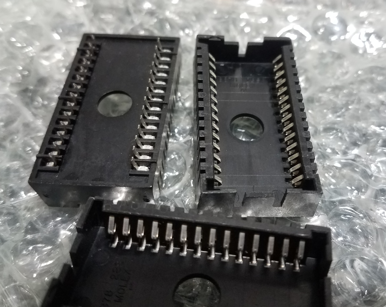
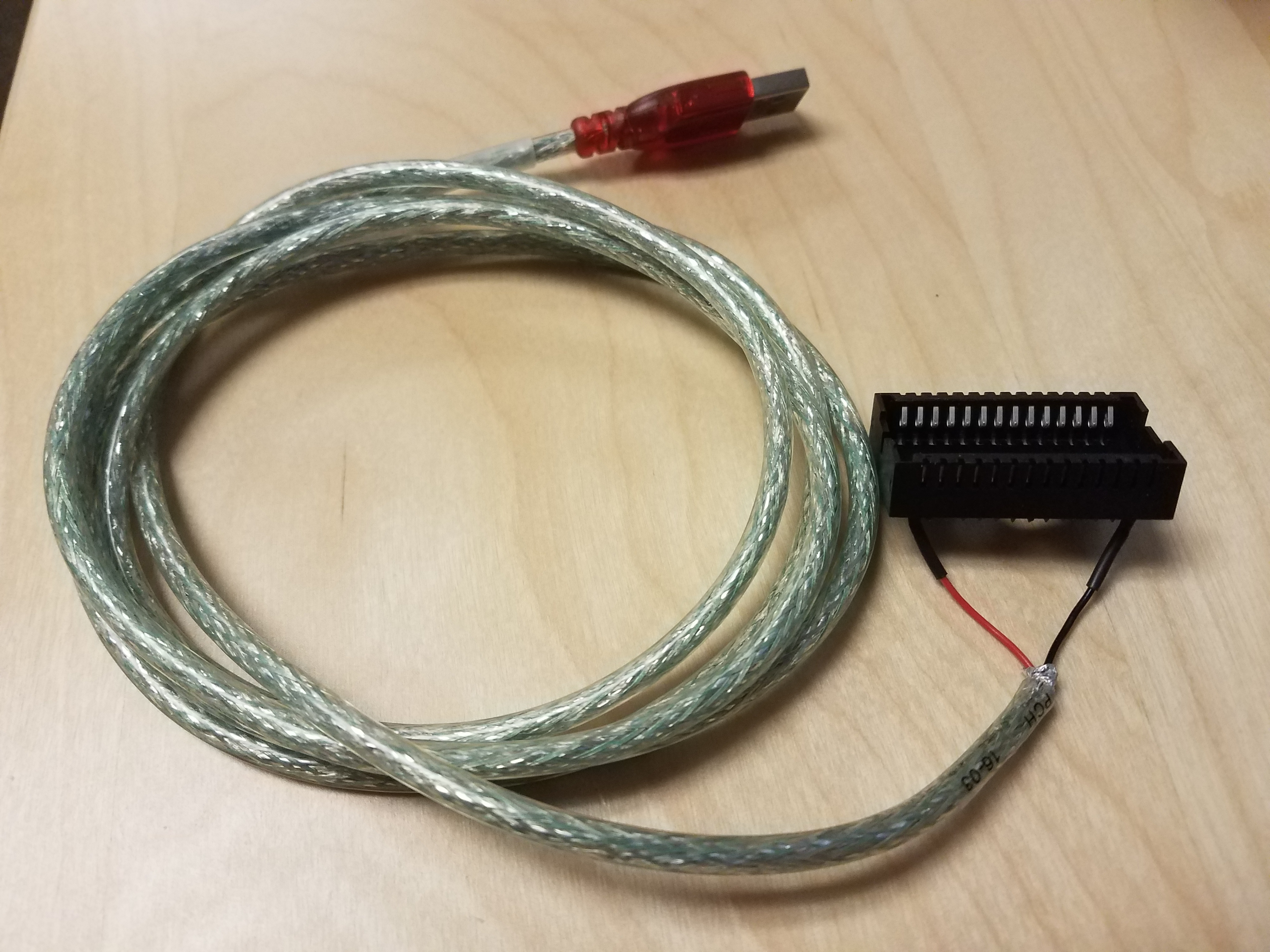
This module socket is the Molex 50-39-5288. Like everything in this project, it’s obsolete and not manufactured anymore.
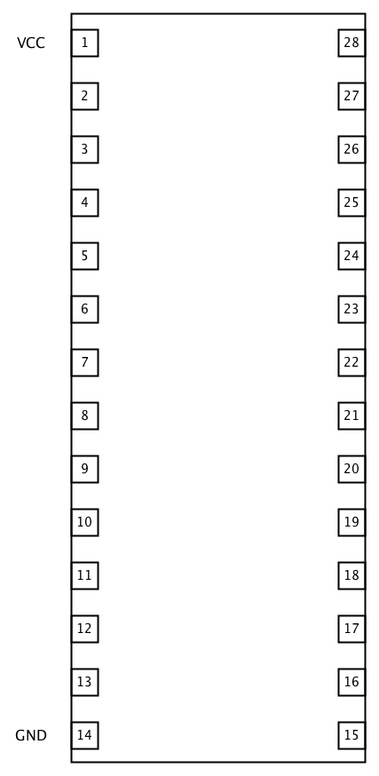
Of course, these special modules didn’t share the normal JEDEC pinout of the common DIP-28 IC ROMs, oh, no. There were a couple of key differences, just to shake things up, I guess. But the only thing I care about at this stage is power and ground, and they’re still located in the usual places. So, if I can get my hands on one of these Molex sockets, I can easily supply 5 volts to the REX while flashing the CPLD. I powered the first 2 boards in the Tandy itself while flashing, and that’s a bit clunky and slightly nerve-wracking. This will be better.
Again, a kind member on the M100 list had a good stash of these sockets and sold me a few really cheap (thanks Brian!) so all I need to do is wire power and ground to it as indicated above and Bob’s my uncle! Luckily, USB is a cheap and easy 5 volt source and I have a ton of cables lying around ready to be hacked.
As I mentioned in my first post, I’ve successfully built a REX based on the plans, parts, and directions available from Stephen and Brian. In the end, the process was not difficult, but it’s not “easy” either, so I thought I would write up some details about the actual construction process.
These were compiled by Brian after his experience building his REX units, and include all the major steps needed to build one. The major steps break down as
Shape the printed circuit (PC) board
Solder the components
Flash the CPLD firmware
Program the flash memory
Getting the Parts
Another great thing Brian has done is locate suppliers for all the parts needed to build a REX. The bill-of-materials (complete list of parts needed) for the REX is actually quite small: 2 resistors, 1 capacitor, a voltage regulator, the CPLD, and the flash chip. However, the CPLD and flash chip can be somewhat difficult to find; both are “obsolete” parts, meaning that they aren’t made anymore. Brian created a single link to the supplier DigiKey which loads your cart with almost all the parts needed. Almost…
The flash chip used by the REX is an “old school” 8 megabit parallel NOR flash. Digikey doesn’t sell any compatible part, but there are still plenty out in the world that are available from other distributors. (We don’t have to take extreme measures to come up with these.. yet.)
The PC board is, perhaps, the easiest of the parts to obtain, since Stephen kindly made the board available from OSH Park, a hobbyist-friendly PCB house. The only minor issue is that they are only available in batches of three. The boards are very inexpensive, so if you’re not building three, it’s no big loss to have a spare board. In fact, having a spare might be really useful, considering the next step…
Shaping the board
image courtesy of Sparkfun.com
The Tandy 100 uses a special option ROM socket that accepts modules with castellated mounting edges, like the photo shown here (borrowed from Sparkfun). Unlike normal DIP ROM chips where pins are inserted into sockets, the Tandy option ROM socket has protruding tabs that connect with the half-moon holes in the castellated board. It’s easy to make a castellated board by just creating plated vias near the edge and then just cut or sand the board down until half of the vias are exposed. Easy… but tedious. I used 80-grit sandpaper to get most of the material off and then finished with something like 160 until I had a nice smooth edge. Then, you need to go over it with a sharp knife and cut off any remaining copper bits that have either folded into the vias or are hanging off the top or bottom.
Soldering to components
The REX is built with entirely surface-mounted (SMT) parts. To someone with little experience with soldering (and even for some with lots of through-hole experience) this can seem daunting. But, like all things that look like “wizard-level” skills, successful SMT soldering is really just a combination of a special technique and the right tools. The technique I use is call “drag soldering” and the special tools are not expensive — just special. Of course, a certain amount of manual dexterity and experience using a soldering iron is required. I plan on making a dedicated post for my soldering technique and experience.
CPLD programming
The CPLD (complex programmable logic device) is a device with logic gates that be programmatically turned into any digital logic circuit that the designer wants. The ship from the factory in a useless state and have to be programmed to do anything useful. The process of “programming” the CPLD is the loading of the designer’s circuit into the device, giving it the intended functionality.
In the case of the REX, Stephen’s CPLD program (released as a .jed file) needs to be loaded onto the REX CPLD. This requires a special (although, again, not expensive) programmer from Xilinx and their programming software. As the REX uses an older CPLD, it only requires older, commonly-available, and inexpensive “Platform USB” programmers, available on eBay for around $25. In my case, though, another fellow on the Model 100 list actually sent me his programmer (along with a complete set of parts) in exchange for assembling some REX units for him. So I’ll be using this to program the REX units.
The REX board includes a set of vias to which the programming cable needs to be attached. They are arranged in an offset configuration which I’ve never seen before, but which is intended to help keep the cable pins in contact with the vias. I connect to these vias, I cut some wire-wrap pins to the correct length to insert into the programming cable and then make contact with the vias.
Flash programming
After the CPLD has been programmed, the REX is a functioning device. But, it order to do anything with it in the Model 100, you need to program some data into the flash memory chip. The design of the REX precludes programming the flash chip with an external programmer, so this is done directly by the Tandy 100 – “in-situ” as it were. The basic process is:
Bootstrap TS-DOS in RAM
Use TS-DOS to load the REX flash .CO program
Run the REX flash .CO, which will load more files from a TPDD device and program them into the flash memory
That’s the basic process. I’ll document the individual stages later.
So, I haven’t had time to even get my Model 100 within 10 feet of a soldering iron to replace that suspect RAM chip. But, that doesn’t mean I haven’t been immersed in the ways of 8-bit computers. Eddie Edwards, on the Club 100 mailing list, posted an absolute treasure trove of Tandy Model 100 and related documents. Unfortunately, he ran into space and bandwidth restrictions with the various free cloud providers, so he couldn’t post it all. Turns out, he has 26 gigabytes!!! of documents – mostly book and magazine scans – that he wants to get archived for good.
The Internet Archive has done amazing work in preserving old computer books, magazines and software, and I figured that this material really belongs there. So, I’ve been working with Eddie to get his collection tagged and uploaded. So far, I have 63 items uploaded, representing something like half of what I’ve gotten from him so far, which is only 11 or so GB. I’m in the process of getting it all into a single collection. The Archive actually makes this a rather painful process, having to email links to their staff who are the only ones who can make a collection it seems.
But, there are some real gems, including this example in April 1984 Portable Computing Magazine of bar-coded BASIC programs. Look Mom – no more type-ins!
Anyway – check out the collection thus far: https://archive.org/details/tandy_books. Note that this is much more than just the material I uploaded, but the most recent 53 items are from this newly-found material.